Table of Contents
ToggleIntroduction
What is a PCB?
A printed circuit board (PCB) is a crucial component in electronic devices, serving as the backbone that connects and supports various electronic components. It is a thin, rigid board made of insulating material with conductive pathways etched onto it, allowing for the interconnection of components and the flow of electrical signals.
Importance of marking points on PCBs
In the complex world of PCB manufacturing and assembly, marking points play a vital role in ensuring accuracy, precision, and quality control. These marks serve as reference points during various stages of the manufacturing process, enabling proper alignment, component placement, and inspection.
Definition of Mark Point
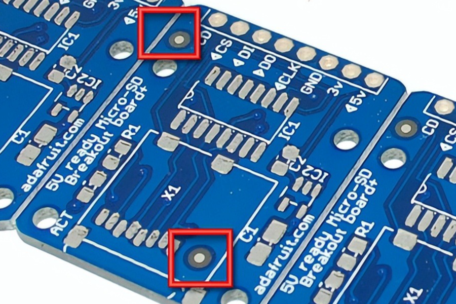
Explanation of mark point
A mark point, also known as a fiducial mark or alignment mark, is a predefined, identifiable mark or pattern placed on a PCB. These marks are strategically positioned and designed to be easily recognizable by automated systems or human operators during the manufacturing and assembly processes.
Purpose of mark points
The primary purpose of mark points is to provide reference points for accurate alignment, enabling precise component placement and ensuring overall quality control. They act as guides for automated pick-and-place machines, vision systems, and other manufacturing equipment, ensuring that components are positioned correctly on the PCB.
Types of Mark Points
Fiducial marks
Fiducial marks are the most common type of mark points used on PCBs. They are typically small, circular or cross-shaped marks placed at specific locations on the board. These marks are recognized by vision systems and serve as reference points for aligning components during the assembly process.
Alignment marks
Alignment marks, similar to fiducial marks, are used for precise alignment during various manufacturing processes, such as panel depanelization (separating individual PCBs from a larger panel), drilling, routing, or other operations that require accurate positioning.
Tooling marks
Tooling marks are typically larger marks or patterns used for aligning and positioning the PCB during manufacturing processes like drilling, routing, or other operations that involve mechanical tools or equipment.
Other types of marks
Depending on the specific manufacturing requirements, other types of marks may be used, such as test points, inspection marks, or identification marks for traceability purposes.
Importance of Mark Points
Accurate component placement
Mark points play a crucial role in ensuring accurate component placement on PCBs. Automated pick-and-place machines rely on these marks to precisely position and orient components, preventing misalignment or incorrect placement, which can lead to manufacturing defects and potential product failures.
Precision during manufacturing
Beyond component placement, mark points contribute to precision during various manufacturing processes, such as drilling, routing, and depanelization. Accurate alignment based on these marks ensures that operations are performed precisely, resulting in high-quality PCBs with minimal defects.
Inspection and quality control
Mark points also facilitate effective inspection and quality control processes. Automated optical inspection (AOI) systems can utilize these marks to accurately analyze and verify the correct placement of components, solder joint quality, and other critical aspects of PCB assembly.
Mark Point Placement
Recommended locations
While the specific placement of mark points may vary depending on the PCB design and manufacturing requirements, there are generally recommended locations to ensure optimal visibility and accessibility. Common placement areas include the corners of the PCB, near the edges, or in designated areas away from components and traces.
Considerations for placement
When determining the placement of mark points, several factors should be considered, such as accessibility for vision systems, avoiding interference with components or traces, and ensuring sufficient contrast and visibility for accurate detection.
Mark Point Design
Size and shape
The size and shape of mark points can vary based on specific requirements and manufacturing processes. Common shapes include circles, crosses, or more complex patterns. The size should be optimized for easy detection by vision systems while ensuring it does not interfere with other PCB features.
Color and contrast
Mark points should have a high contrast against the PCB substrate to ensure easy detection and recognition. Commonly used colors include copper (for bare PCBs) or contrasting colors like white or black (for solder mask or silkscreen layers).
Durability and permanence
Mark points should be designed to be durable and permanent, withstanding various manufacturing processes and environmental conditions. They should not be easily damaged or obscured, as this can compromise their effectiveness as reference points.
Mark Point Inspection
Manual inspection
In some cases, manual inspection of mark points may be necessary, particularly during prototyping or small-scale production runs. Human operators can visually inspect the presence, quality, and accuracy of mark points using magnification tools or microscopes.
Automated optical inspection (AOI)
Modern PCB manufacturing heavily relies on automated optical inspection (AOI) systems for efficient and accurate mark point inspection. These systems use advanced imaging and vision algorithms to automatically detect, analyze, and verify the presence and quality of mark points on PCBs, ensuring compliance with design specifications and quality standards.
Mark Point Best Practices
Design guidelines
Adhering to industry-standard design guidelines and recommendations is crucial when incorporating mark points into PCB designs. These guidelines cover aspects such as mark point size, shape, placement, and specifications for various manufacturing processes and applications.
Manufacturing guidelines
During the manufacturing process, following best practices for mark point creation and preservation is essential. This includes proper solder mask or silkscreen application, ensuring mark points are not obscured or damaged during subsequent processes, and maintaining consistent quality across all PCBs.
Inspection guidelines
Implementing robust inspection protocols and adhering to industry-standard guidelines for mark point inspection is vital for ensuring quality control. This includes defining acceptable tolerances, establishing clear pass/fail criteria, and implementing corrective actions when deviations or defects are detected.
Conclusion
Summary of key points
Mark points are essential features on PCBs that serve as critical reference points for accurate component placement, precise manufacturing processes, and effective quality control. By understanding their importance, types, placement considerations, design principles, and inspection methods, manufacturers can ensure high-quality PCB production and reliable product performance.
Importance of mark points for PCB quality
Neglecting the proper implementation and inspection of mark points can lead to costly manufacturing defects, product failures, and potential safety risks. As such, mark points are a fundamental aspect of PCB design and manufacturing, playing a crucial role in maintaining the high standards of quality and reliability expected in the electronics industry.
FAQs
Can mark points be added to an existing PCB design?
Yes, mark points can be added to an existing PCB design, provided there is sufficient space and clearance from other components and traces. However, it is generally recommended to incorporate mark points during the initial design phase for optimal placement and integration.How many mark points are typically needed on a PCB?
The number of mark points required on a PCB can vary depending on the size, complexity, and manufacturing requirements. As a general guideline, at least three mark points are recommended for accurate alignment and positioning, with additional marks often used for larger or more complex PCBs.Are there different standards or specifications for mark points in different industries?
Yes, different industries or applications may have specific standards or guidelines regarding the design, placement, and inspection of mark points on PCBs. For example, the aerospace or medical device industries may have stricter requirements compared to consumer electronics.Can mark points be reused or modified during PCB rework or repair?
It is generally not recommended to modify or reuse existing mark points during PCB rework or repair processes. Any alterations to mark points can potentially compromise their accuracy and reliability, leading to alignment issues and potential defects. In such cases, it is advisable to follow the manufacturer’s guidelines or consult with experts.Are mark points required for all PCB manufacturing processes?
While mark points are essential for many PCB manufacturing processes, such as component placement, depanelization, and automated optical inspection, there may be instances where they are not strictly required. For example, in some manual assembly processes or simple PCB designs, mark points may not be necessary. However, incorporating mark points is still considered a best practice for quality control and ensuring manufacturing precision.